Wafer Testing (also known as EDS - Electrical Die Sorting) is an elementary step in the production of any semiconductor structure and process technology. More specifically, after the integrated circuits are manufactured and before they are separated from the wafer, all individual electrical contacts are tested for functional defects according to specific electrical test patterns. This integrated circuit test (also known as CP - Circuit Probe) is performed by automated test units and requires a high level of reliability in the interface between the tester and the wafer contact pad. This interface is provided by probe cards and probe needles.
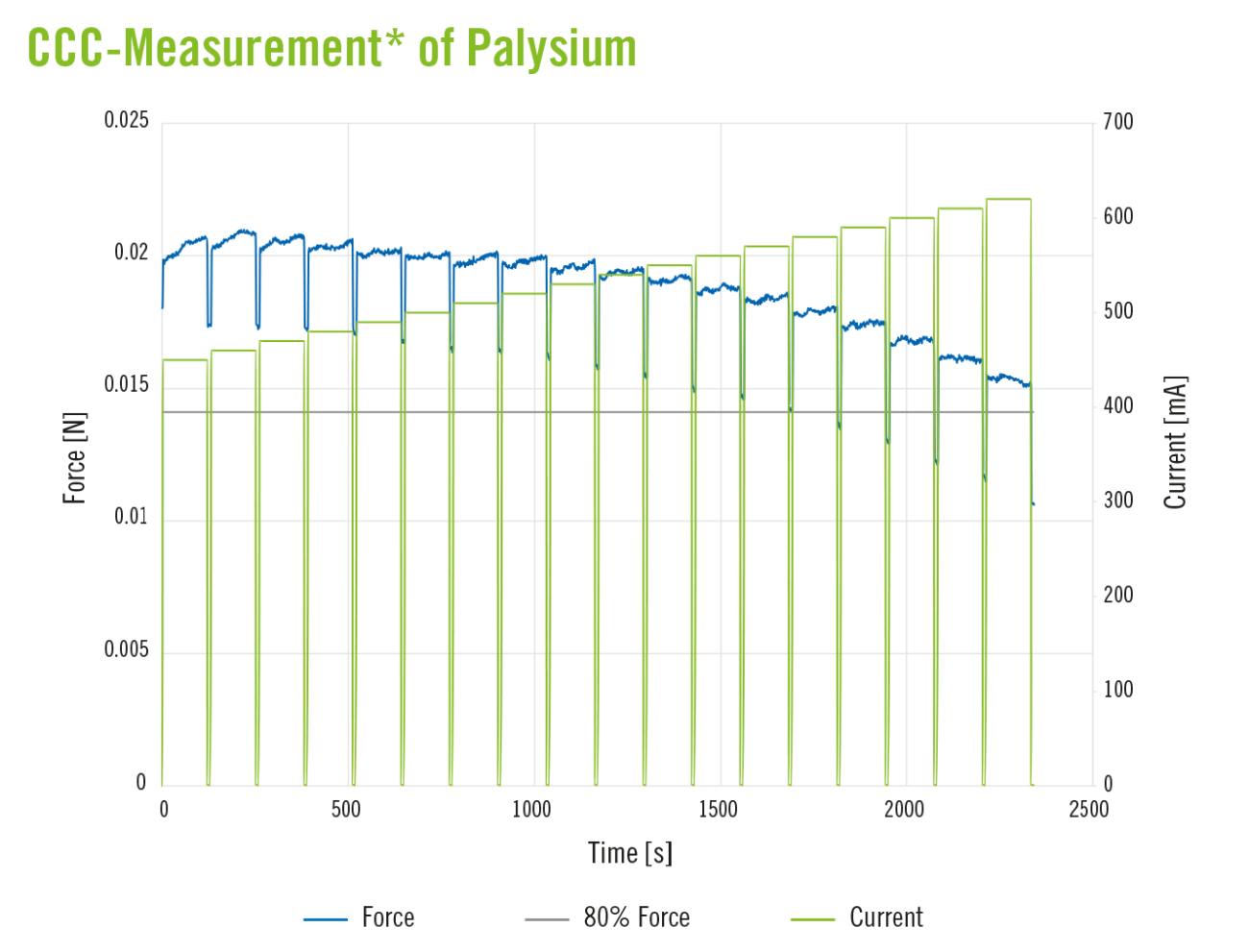
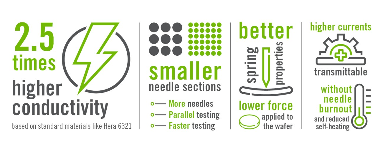
High demands are placed on the probe needles in the probe card. Due to the minimal pitch distances between the individual contact pads, they must be extremely straight and have excellent electrical conductivity. In addition, they must be sufficiently elastic and have good mechanical strength even at high temperatures to be used over many load cycles and touchdowns. The most important metric for probe card efficiency is to reduce the cost per test, the time per test and to increase the number of parallel tests while minimizing contamination (low contact resistance CRes).


