Advanced Packaging Application Center in Singapore

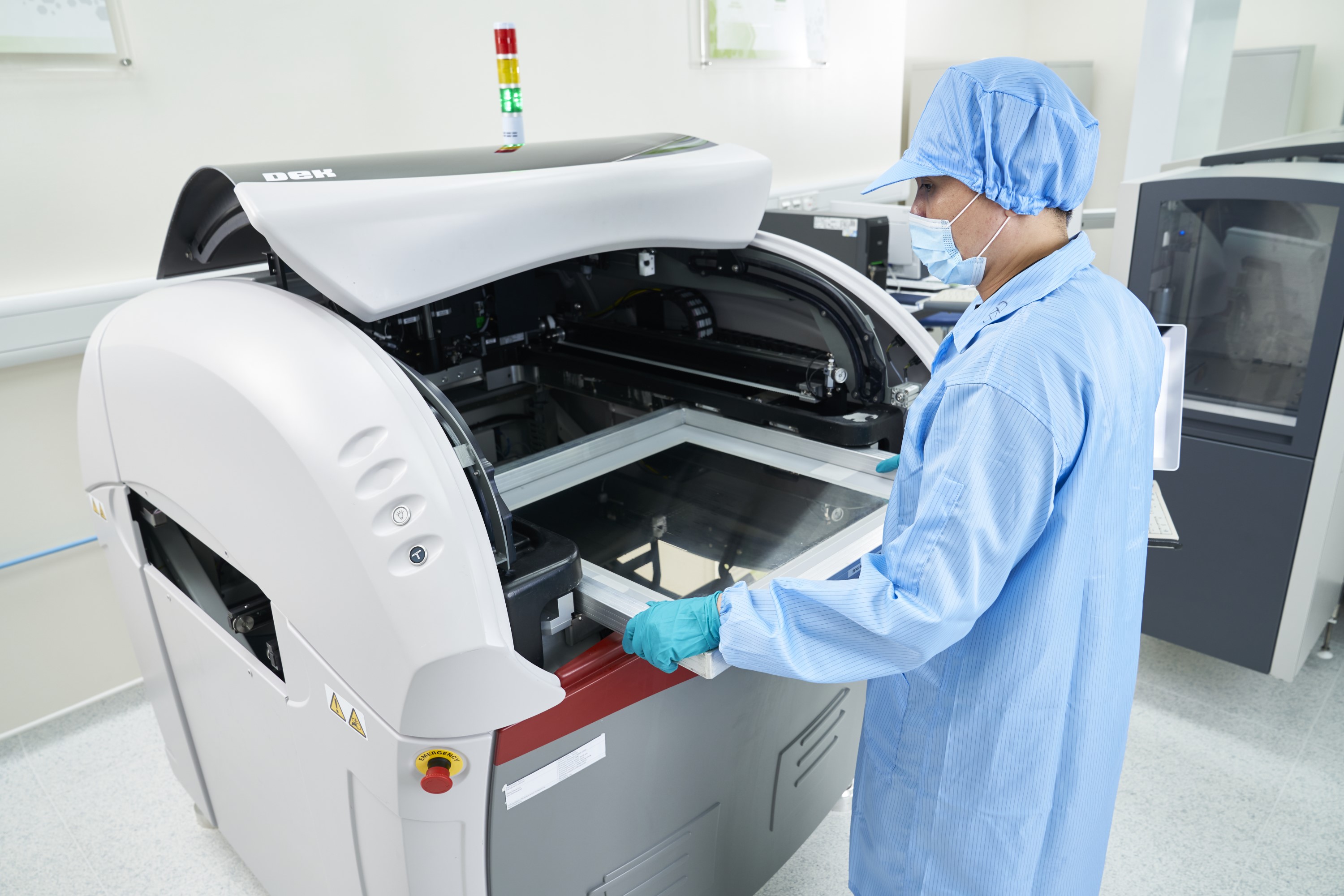
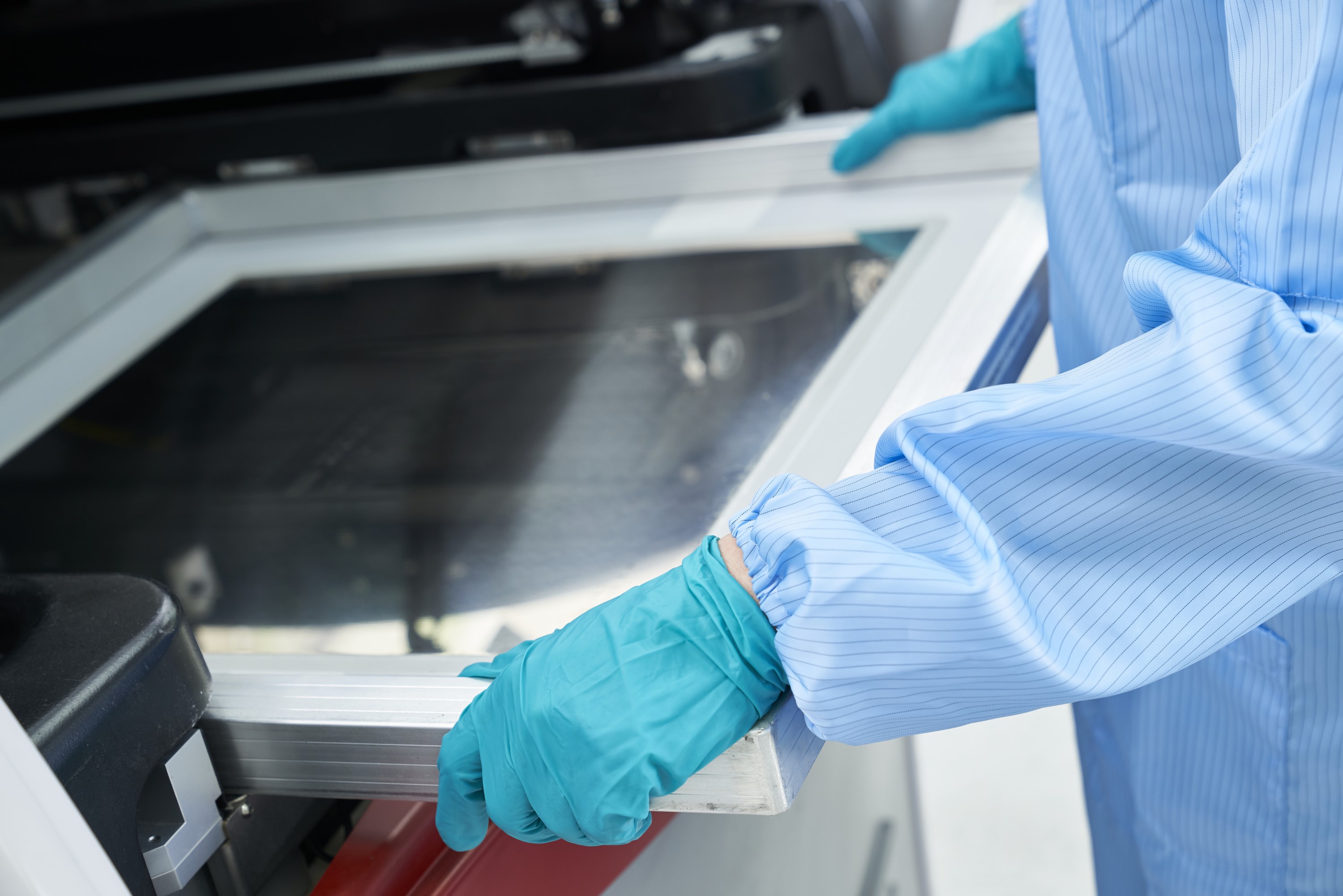
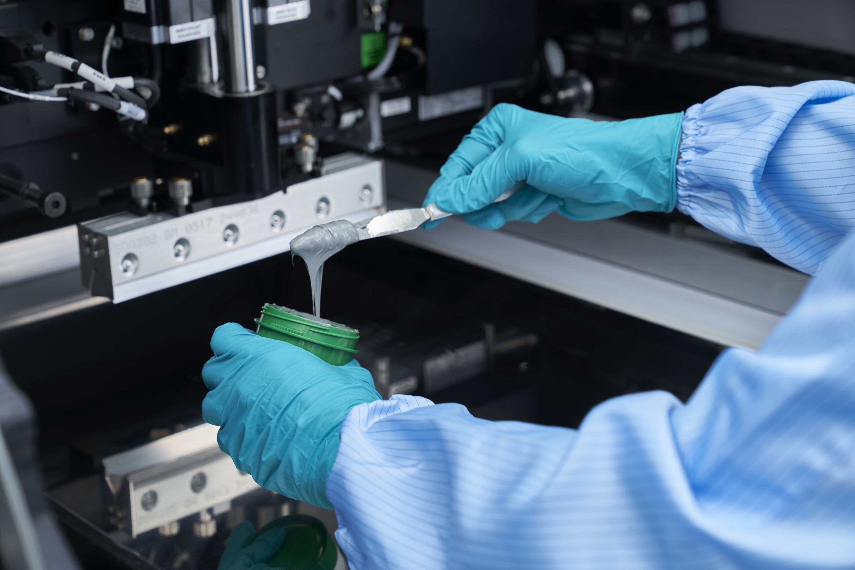
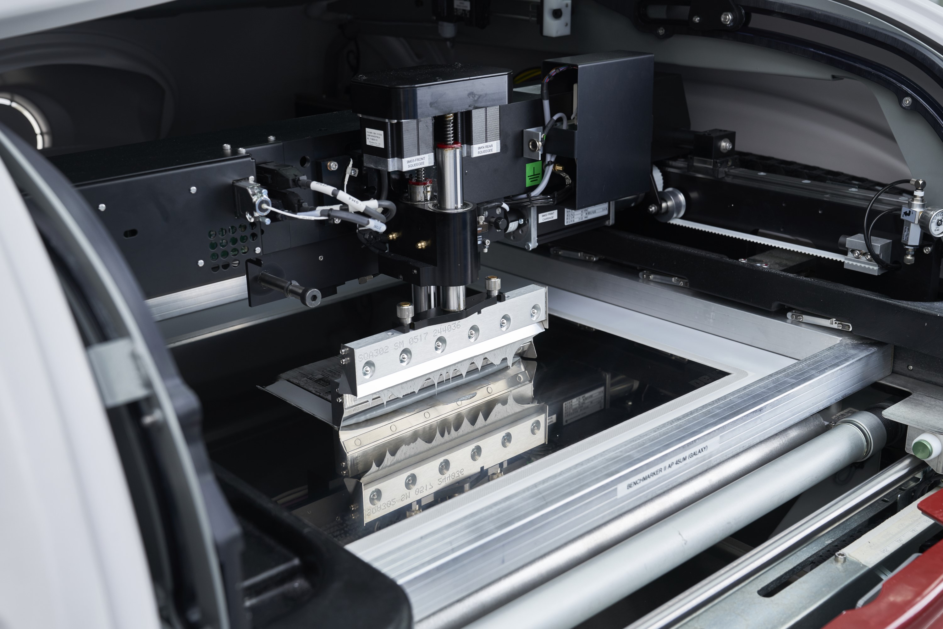
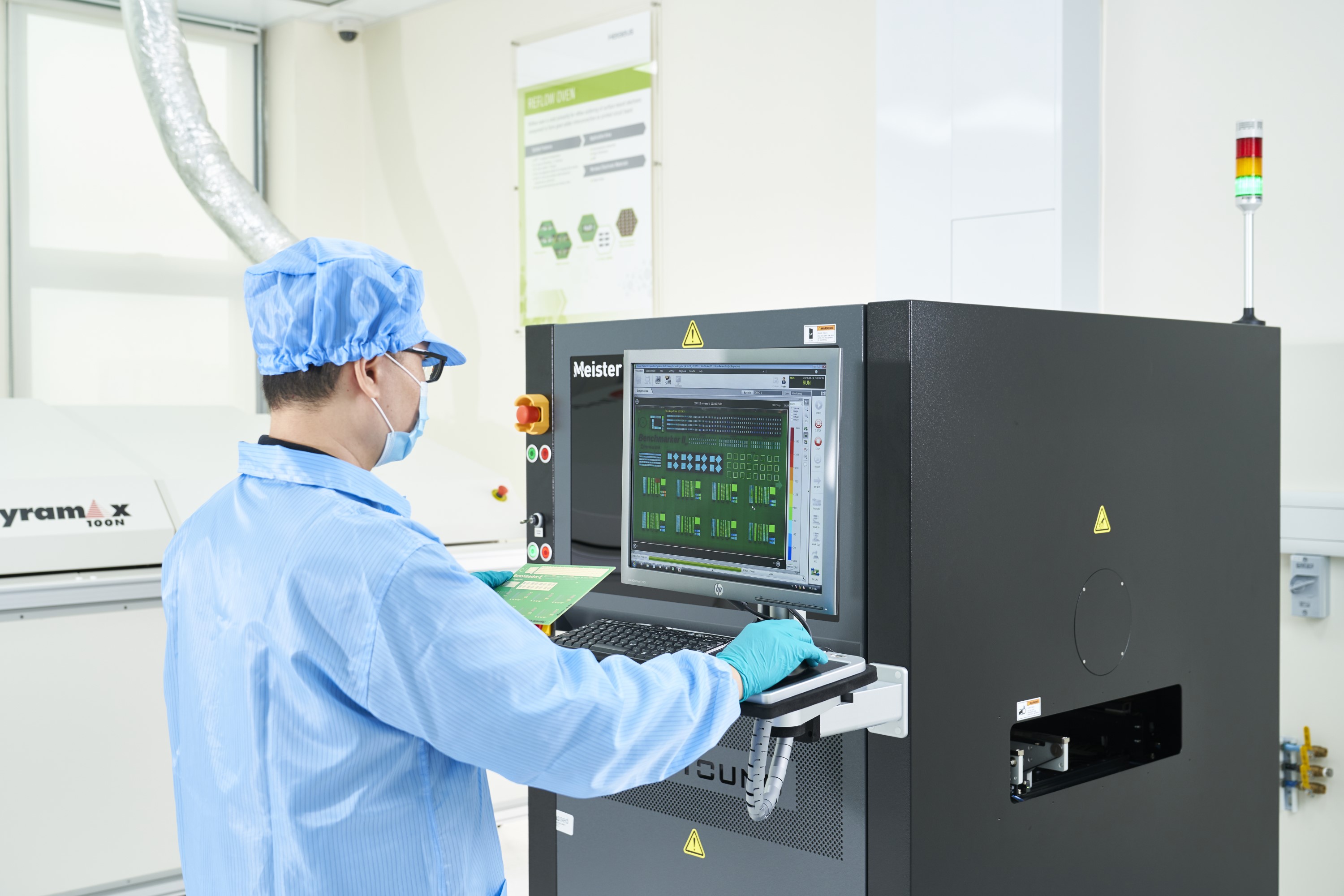
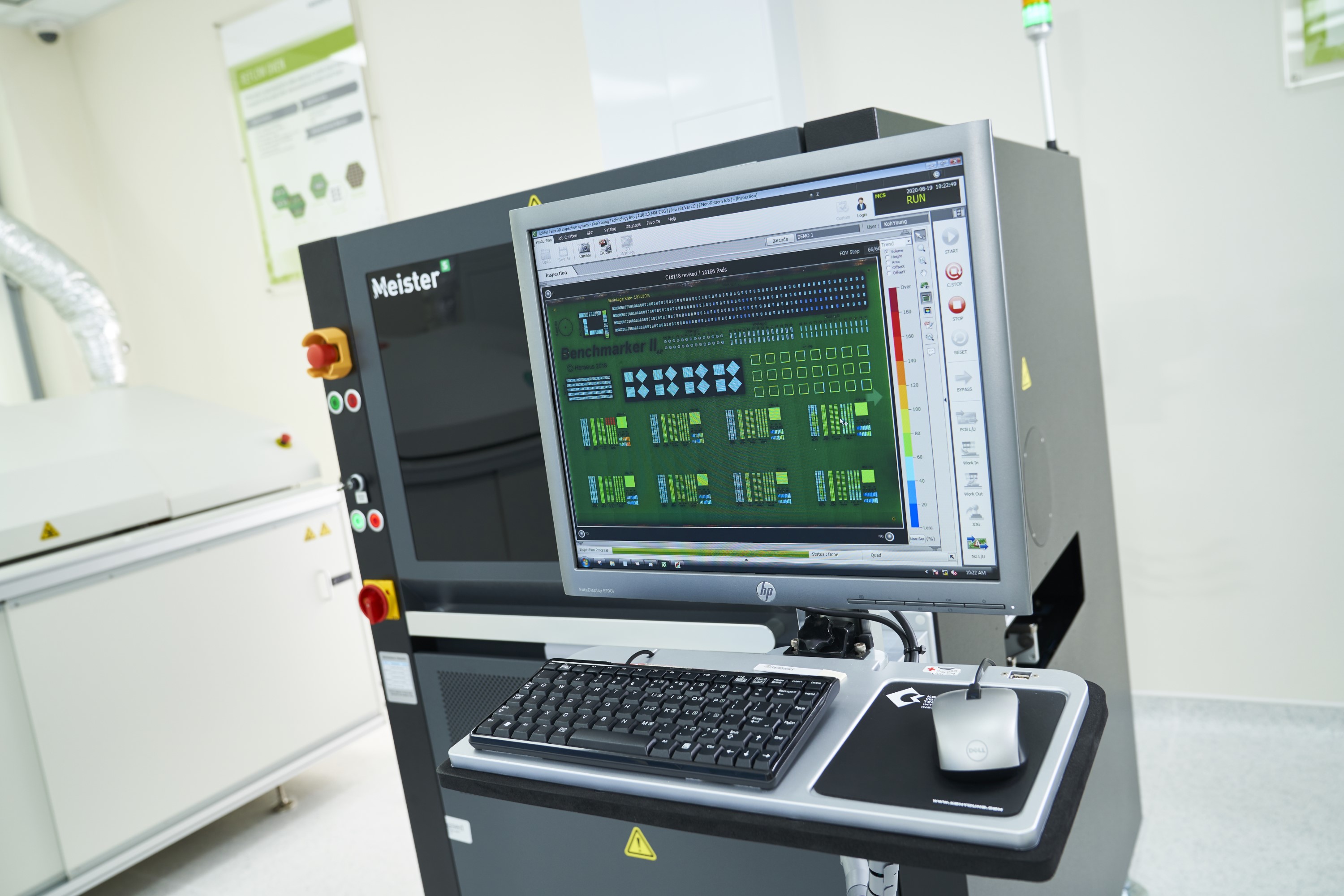
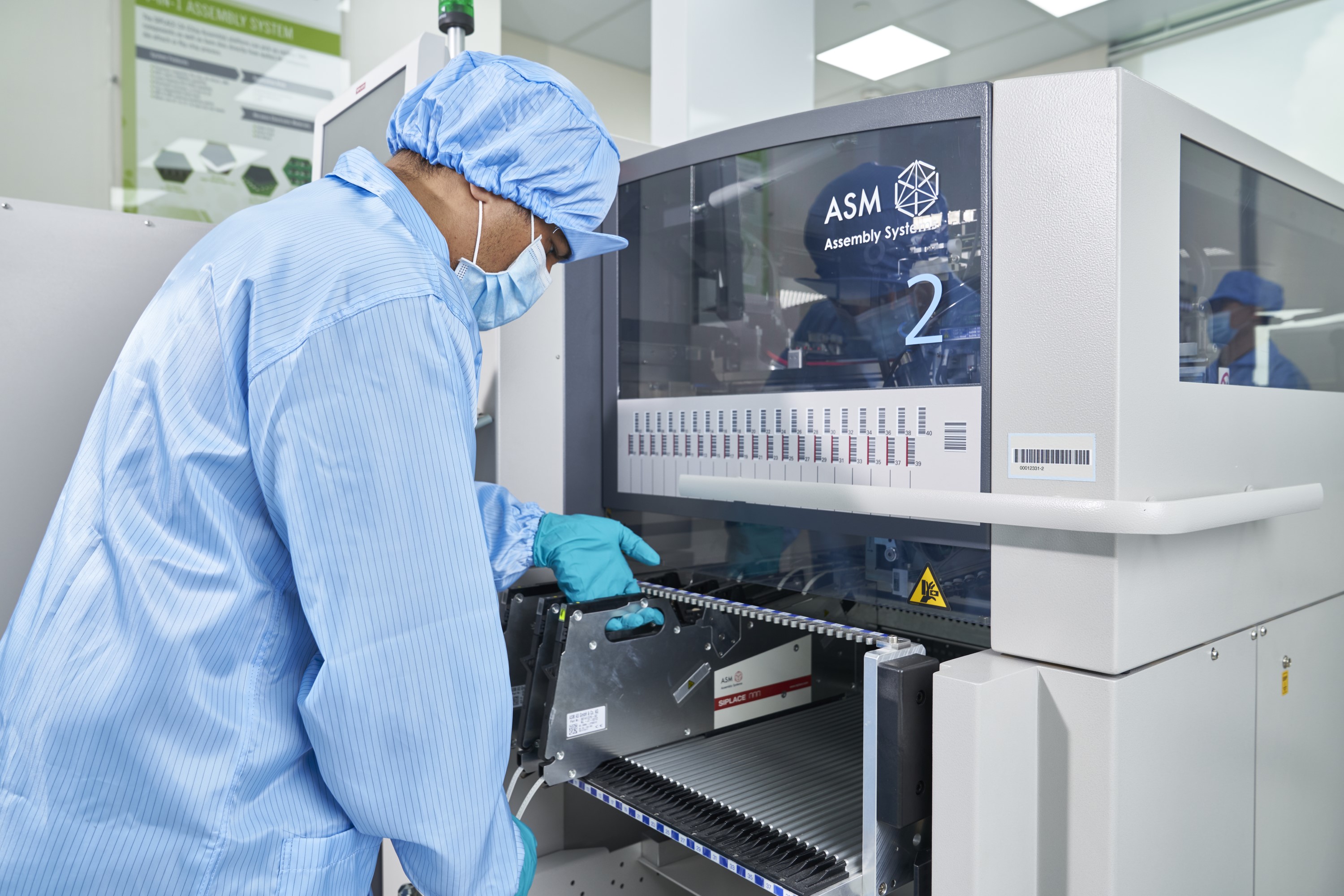
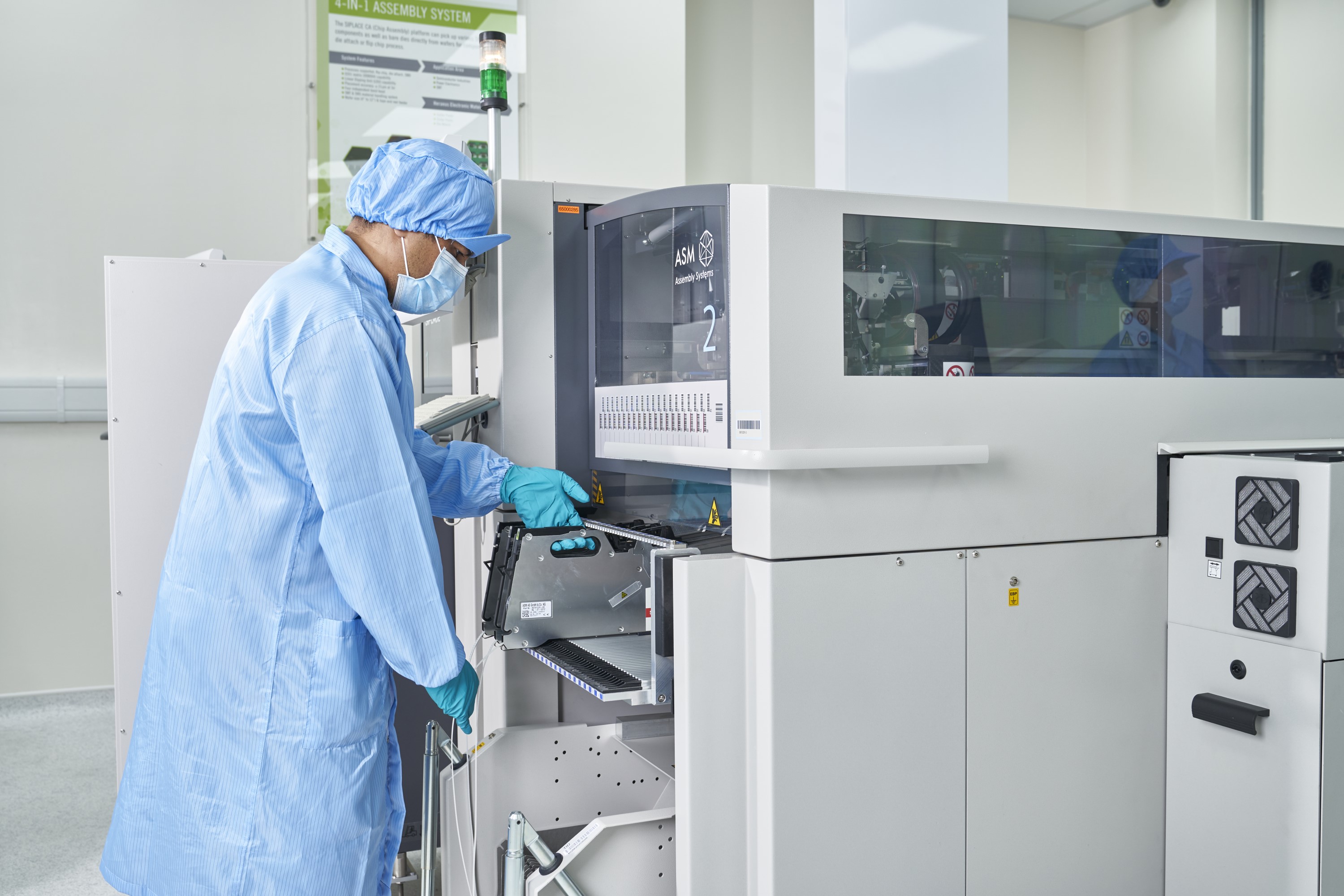
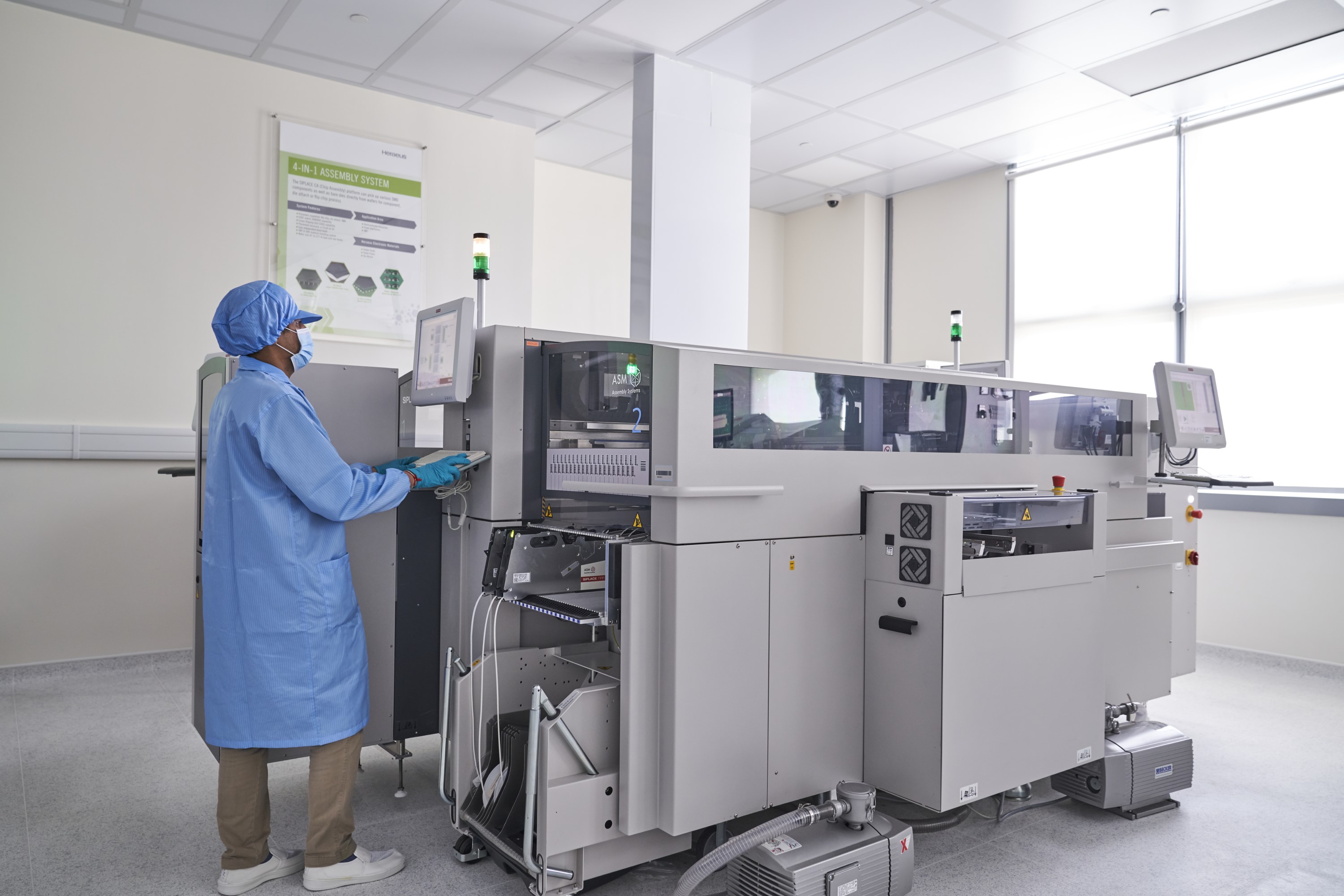
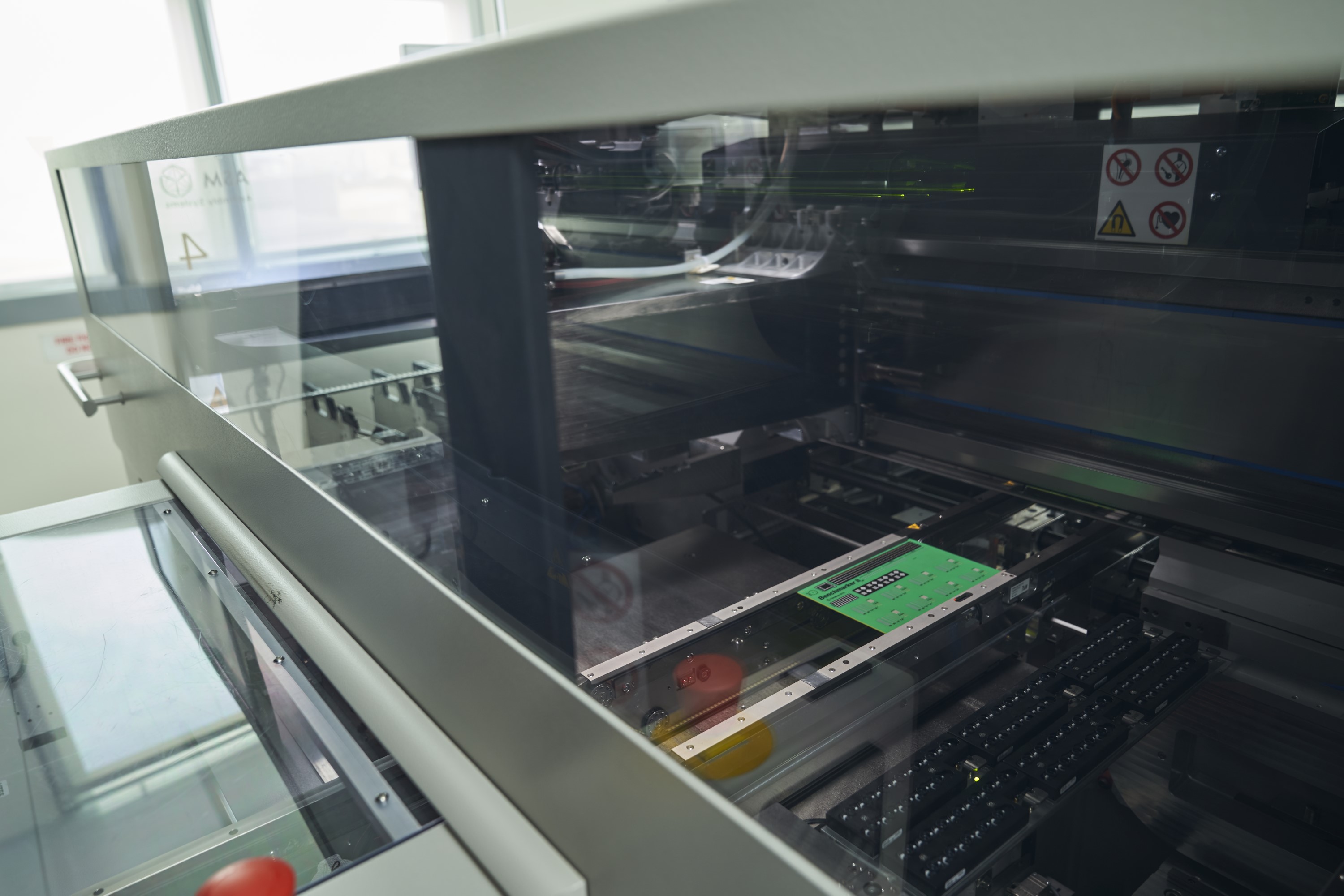
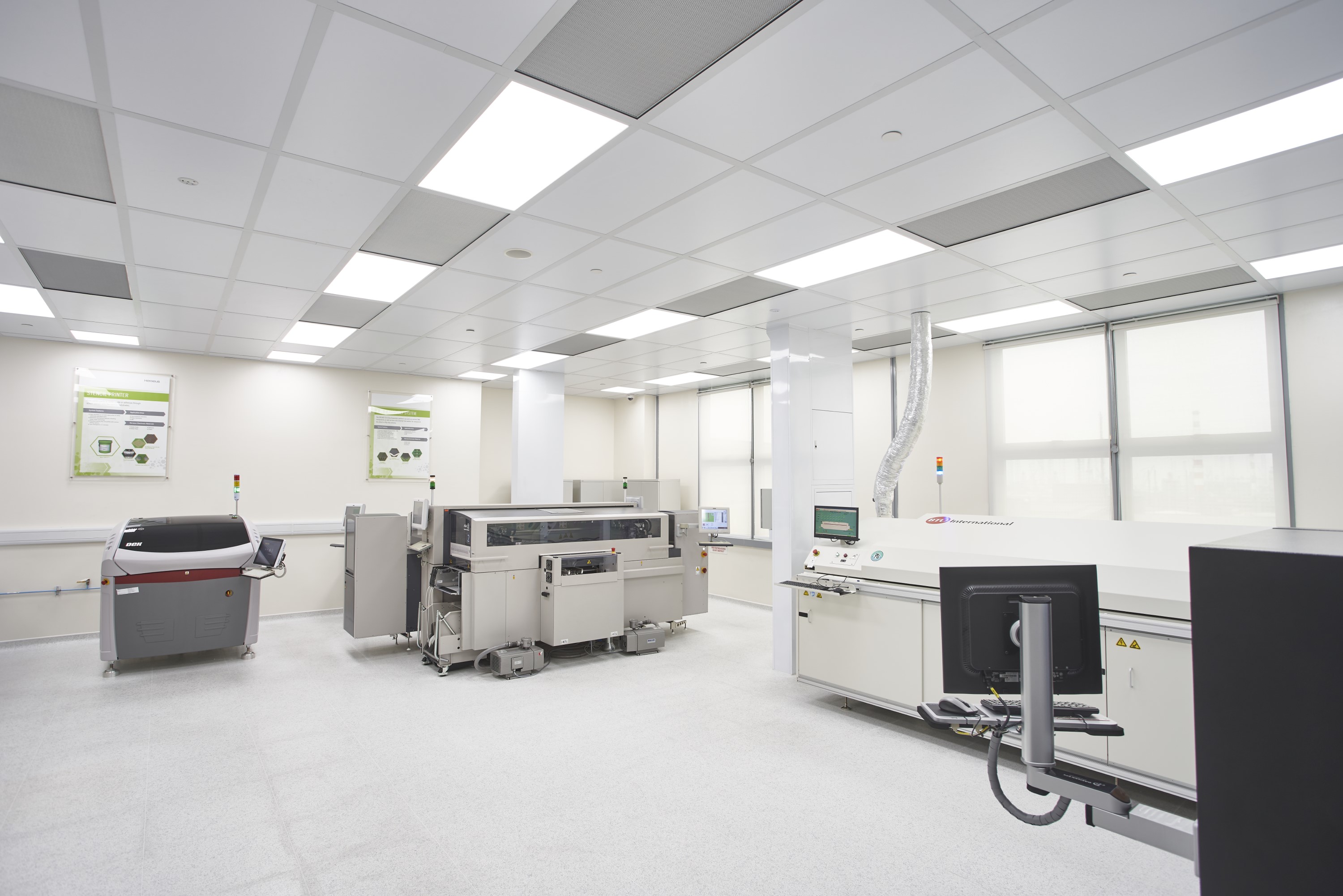
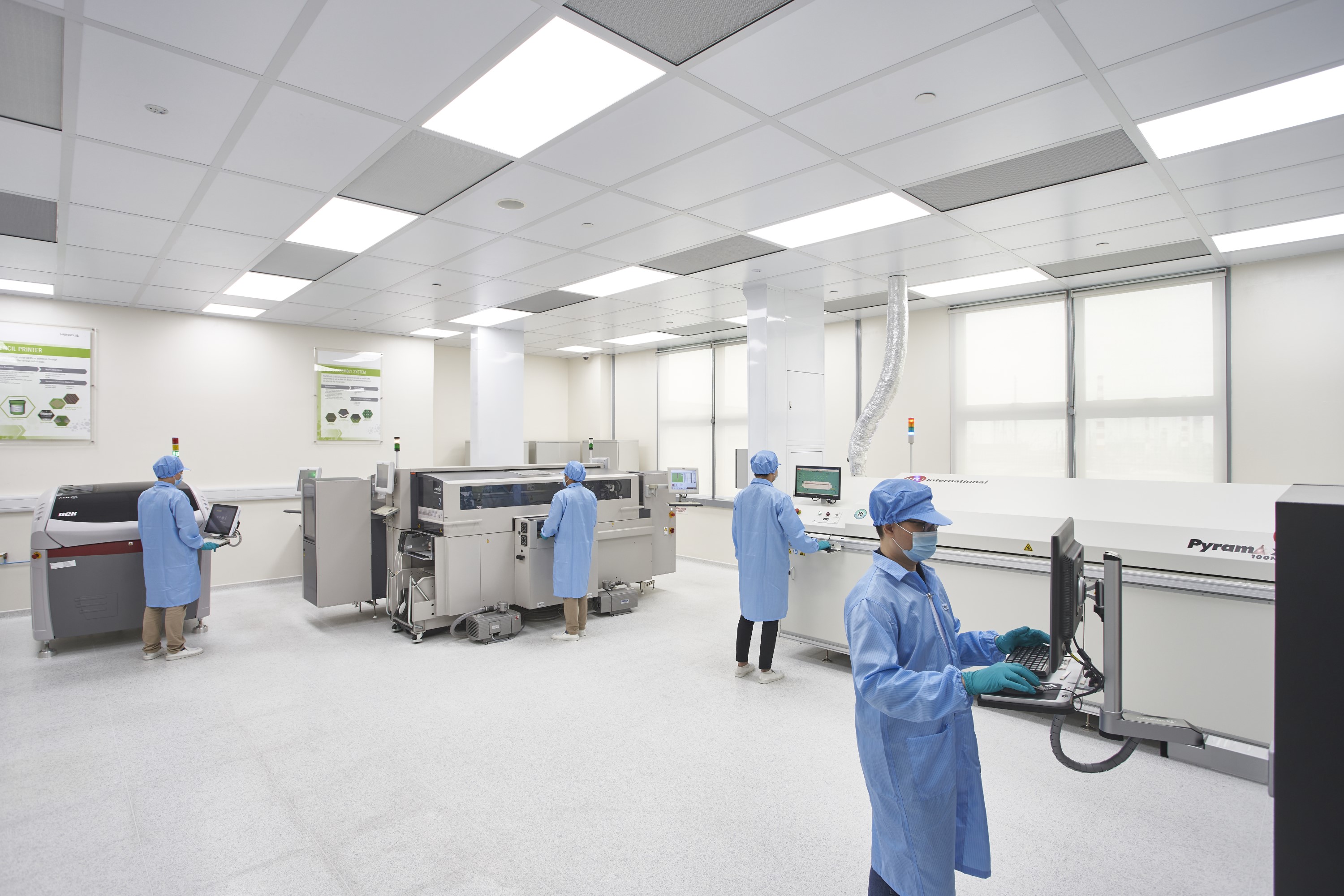
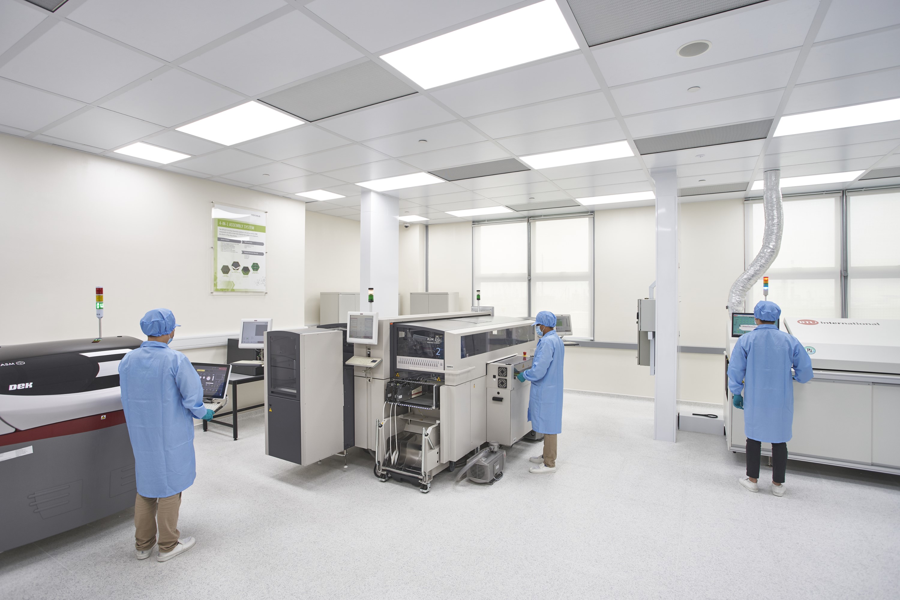
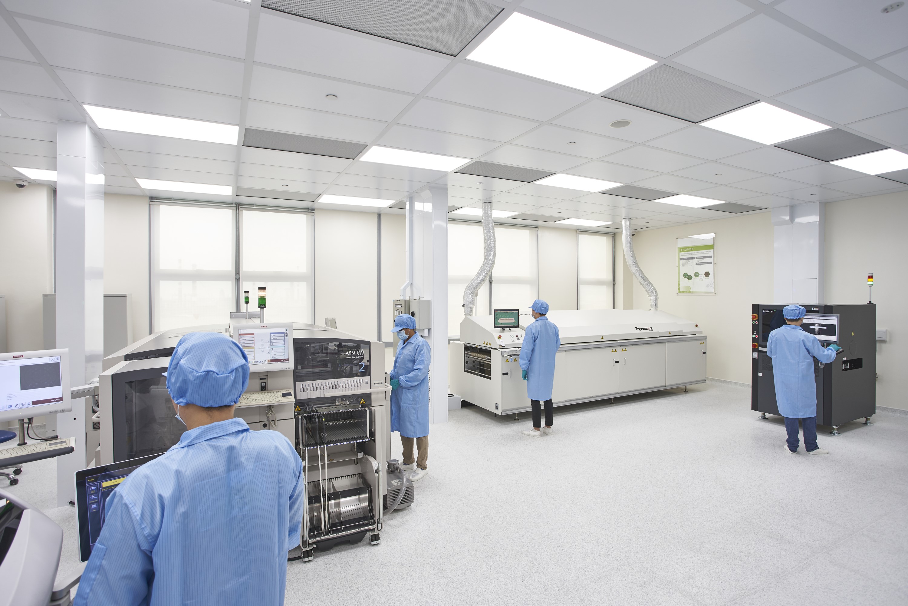
The state-of-the-art application center in Singapore offers comprehensive application services aimed at being a full-fledged advanced packaging hub. With our customers in mind, the application center is equipped with the latest and modern equipment to deliver a quick response in test options and results. In addition to the application center, the climate-controlled cleanroom has a unique ability to match the customers' environmental conditions regardless of region. The cleanrooms’ comprehensive state-of-the-art equipment provides the highest customer support level - due to closer proximity to the customers' production line. Our engineers also work on product development, prototype design, performance testing, and material system qualification for the advanced packaging industries.

Our optimum infrastructure and comprehensive equipment have shortened the product development cycles through our application expertise in matching materials and a better success rate of first-time development. Our experienced engineers in packaging solutions will significantly benefit you and your team to succeed.

Your benefits at a glance

  • Access to the state-of-the-art assembly line
  • Local technical experts solving your complex systems and materials challenges
  • Future Training Programs: advanced packaging, solder & sinter die attach product and process training programs at our facility, hands-on and practical trainings for your teams
  • Process optimization for improved reliability
  • Reduced development risks
  • Shortened development cycles and faster time to market
  • Higher first-time success rates
  • Efficient use of resources in the value chain

You have not agreed to all cookies, which limits the use of the website and performance. To be able to use our website to its full extent, please agree to all cookies. You can change your preferences in the cookie settings.

You can change your preferences in the cookie settings.

Our Engineering Services in Singapore

  • Solder & Sinter paste: Ultra fine pitch stencil printing, dispensing, pin transfer, stamping, jetting
  • Component attach (008004)/ Die attach ( 500 µm to 10 mm die size) / Cu pillar attach / Flux dipping
  • Multi stacked-die fine wire bonding (0.6 mil to 2.0 mil)
  • SEM/EDX Spectroscopy – (Scanning Electron Microscopy with Energy Dispersive X-Ray)
  • X-Ray
  • 3D SPI
  • FTIR – Fourier Transform Infrared Spectroscopy
  • TGA – Thermo Gravimetric Analysis
  • DSC – Differential Scanning Calorimetry
  • Zeta potential on powders
  • Wire bonding pull & shear testing, hot die shear
  • Micro hardness
  • Cross sectioning & analysis
  • Stress and strain analysis
  • Reliability tests (HTS/µHAST)

Learn more about our services in the other application centers.